
What Is a Prototype PCB Used For?
Prototype PCB
Printed circuit board prototypes serve a variety of purposes. They help designers verify that their products function correctly and efficiently, and they provide insights that can improve PCB design and manufacturing processes. These benefits are critical for ensuring that final products meet customers’ expectations and reliability requirements. In addition, prototyping can save time and money compared to discovering issues after mass production.
The prototyping process is an essential phase in the design of a new electronic product. Throughout this process, engineers test and refine their ideas with various types of printed circuit board prototype, including both simple and complex boards. Prototypes also allow for iterative improvements, which can lead to superior designs that are more efficient and effective in the real world. Moreover, prototypes can also serve as valuable tools for communicating with stakeholders and gaining necessary approvals.
In order to create a PCB, the designer must first conceptualize its overall functionality and structure. This can be done with a PCB design software suite, which allows the designer to map out the layout of the board and determine what electronic components, like chips and sensors, are required to make the device work as intended.
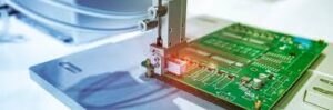
What Is a Prototype PCB Used For?
After the design is complete, it must be translated into a prototype PCB layout using advanced design software. The layout identifies the physical placement of the components and routing of the conductive pathways across the board. This can be difficult, as it requires careful consideration of factors such as component size and positioning, signal integrity, and thermal management. The layout is then sent to a prototype PCB manufacturer for fabrication.
The fabrication process involves applying a layer of copper to the surface of the board. Then, using photolithography or CNC milling techniques, the copper is etched to form the conductive pathways as specified in the design. The board is then cut and drilled to create holes for the components, and the components are placed and soldered onto the circuit board.
PCB prototyping comes with various challenges, including managing design complexity, minimizing manufacturing costs, and adhering to tight project timelines. With the increasing demand for smaller, faster, and more efficient electronics, designers often face the added pressure of incorporating advanced technologies like surface-mount components, high-speed circuits, and rigid-flex designs. To address these challenges, many designers collaborate with specialized PCB manufacturers who offer rapid prototyping services. These services leverage cutting-edge equipment and expertise to deliver high-quality prototypes quickly and efficiently.
The importance of PCB prototyping cannot be overstated in the modern electronics industry. It not only ensures the functionality and reliability of the final product but also contributes to faster time-to-market and reduced development costs.
The final stage in the prototyping process is to conduct rigorous testing and evaluation. Common tests include thermal, EMI, and environmental testing. Thermal testing assesses how well the board can dissipate heat, while EMI testing checks for electromagnetic interference. Environmental testing evaluates the ability of the board to withstand different temperature and humidity conditions.